Abstract
In the present paper a new version of multilevel inverter is investigated. This new version is based on hybrid association of commutation cells with H-bridge cells. The association allows a significant reduction of the volume of the capacitors. In fact, presented topology allows us to work on higher input voltage levels with the same power switches. This new version is generally called as SCMI (stacked cascade multilevel inverter). The proposed inverter has potential to generate high quality waveforms, reduction in switching frequency, capable to operate at higher voltage levels and finally utilizes minimum number of switching components. The presented version of SCMI is simulated in Matlab-simulink and further, experimental validation is carried out in the laboratory with prototype setup.
Keywords
Multilevel inverter ; SCMI ; High quality waveforms
1. Introduction
Multilevel converters gained popularity and increased attention in industry and academia as one of the preferred choices of electronic power conversion for high-power applications [1] , [2] and [3] . They have fruitfully made their way into the industry and thus can be considered a mature and proven technology. Currently, they are commercialized in standard and customized products that power a wide range of applications, such as pumps, fans, compressors, extruders, grinding mills, rolling mills, conveyors, crushers, blast furnace blowers, gas turbine starters, mixers, mine hoists, active and reactive power compensation, marine propulsion, high-voltage direct-current (HVDC) transmission, hydro pumped storage, wind energy conversion, and railway traction, to name a few [4] , [5] and [6] . Converters for these applications are commercially offered by a growing group of companies in the field [7] and [8] . Although it is a proven technology, still, multilevel converters present a great deal of challenges, and even more importantly, they offer such a wide range of possibilities that their research and development is still growing in depth and width. Researchers and industries all over the world are working hard in contributing to further improve the energy efficiency, simplicity, reliability, power density, and cost effectiveness of multilevel converters, and broaden their application field as they become more attractive and competitive than classic topologies.
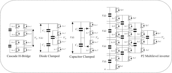
In the recent past [9] , [10] and [11] , different multilevel inverters came into existence. Some of the prominent multilevel based archetypes are Neutral point clamped (NPC), Flying capacitor (FC) and Cascade H-bridge (CHB) multilevel inverter and P2 multilevel inverter. Fig. 1 shows the classical and major multilevel topologies. Although these classes of inverter topologies are prominent in high power applications, they still have some demerits like usage of many switching components, reliability, and EMI problems. To evade these problems research community is in hunt of new kind of architectures and switching techniques. However, in this scenario, a new version of multilevel architectures is evolved, and this structure is quite versatile when compared with traditional multilevel inverter. The origin of this structure is from SMC (stacked multicell) converters. After major modifications in FC converters, SMC is evolved. However, after finite modification in the SMC and cascade multilevel inverter a new version is introduced, i.e. SCMI (stacked cascade multilevel inverter). This paper is completely devoted to investigate SCMI performance. The key reasons for the investigation on this archetype are as follows: (1) they have the capability to handle high voltage power applications, (2) the architecture is modular (in case of any fault it is easily replaceable), (3) generation of high quality waveform (as storage elements are involved). In fact, all these features make this structure to be a good competitor for other multilevel inverters in the power market.
|
|
|
Fig. 1. Details of traditional multilevel inverter.
|
Aforementioned, SCMI is based on a hybrid association of commutation cells and allows a significant reduction of the volume of the capacitors. Thus SCMI gains an inherent potential to allow us to work on higher input voltage levels with the same power switches. As SCMI uses imbricate cell topology, we obtain a strong improvement of the waveforms at the output of the converter. Another remarkable issue is, this new version has the capability to generate higher number of levels with less number of switching components. To confirm the theoretical findings presented, adequate simulations are performed with Matlab-Simulink and further, experimental validation is carried out in the laboratory with Prototype setup.
2. Traditional multilevel inverter
2.1. Cascade multilevel inverter
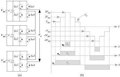
Architecture shown in Fig. 2 is a series H-bridge inverter that appeared in 1975, but a number of recent patents have been obtained for this topology as well. Since this topology consists of series power conversion cells, the voltage and power level may be easily scaled. Numerous advantages have been figured out using this topology, which are extensively used in medium and high power applications. Examining Fig. 2b , the output phase voltage can be expressed as v = v1 + v2 + v3 ; this is because all the inverters are connected in series. Each single-phase full bridge inverter can generate three level outputs vdc , 0 and –vdc , and this is made possible by connecting the DC sources sequentially to the AC side via the four switching devices. Minimum harmonic distortion can be obtained by controlling the conducting angles at different inverter levels. Further, to improve the quality of the synthesized output waveform several PWMs are also available.
|
|
|
Fig. 2. (a) Cascade H-Bridge multilevel inverter. (b) Key waveform for seven-level inverter.
|
Thus this structure is quite renowned and gained popularity for its functions and features. Some of the attributes of this converter, to name a few, are its being cost-effective, efficient, possible to modularize circuit layout and easy to pack, because each level has the same structure, and there are no extra clamping diodes or voltage balancing capacitors. However, CHB has the greatest disadvantage, i.e. it uses separate DC source for each H-bridge cell. Provision of separate DC source for each H-bridge cell not only increases cost but also affects the reliability of the converter.
2.2. Flying capacitor
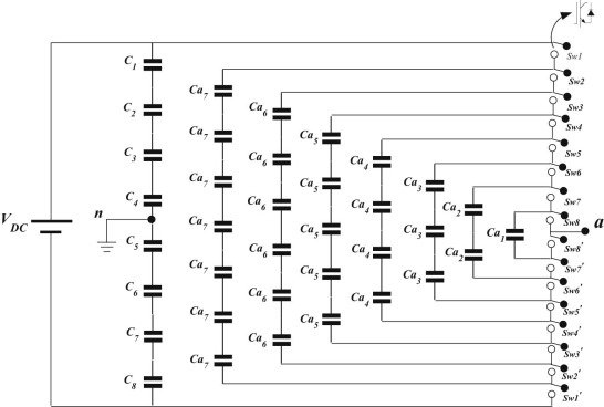
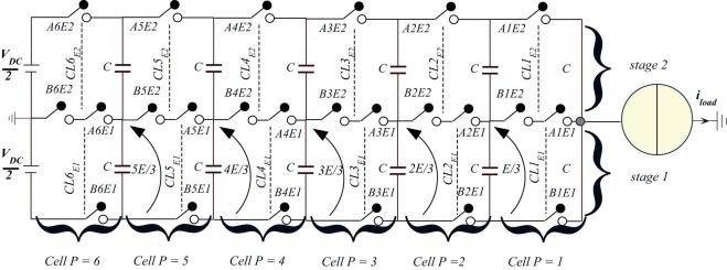
Before going to new version, lets have an idea about the flying capacitor and stacked multicell inverter. Fig. 3 shows five-level flying capacitor (FC) architecture. On observing this architecture, large numbers of capacitor are utilized in the structure. The Flying Capacitor topology was introduced by Meynard in 1992 [12] ; this topology is based on the connection of two level cells, as shown in Fig. 4 . Due to this reason the maximum number of levels at the output of this converter is:
|
|
( 1) |
where m is number of levels and n is the number of cells connected.
|
|
|
Fig. 3. Details of nine-level flying capacitor inverter.
|
|
|
|
Fig. 4. Details of 6 × 2 (nine-level) stacked multicell inverter.
|
For a proper operation, the DC-link voltage on each cell must be accomplished with
|
|
( 2) |
where i represents the number of capacitors and n is the number of cells.
Fortunately, this condition is reached by the inverter itself if the modulation strategy applies the redundancy states in an alternate way. A main advantage of FC over CMI (shown in Fig. 2 ) converter is that FC does not require a complex input transformer, in case of internal fault.
2.3. Stacked Multilevel Converter (SMC)
Fig. 4 demonstrates the SMC architecture. This class of topology was developed at the LEEI in the beginning of year 2000. The alternative topology based on the FC is the Stacked Multilevel Converter [12] and [13] . This topology is composed of p × n commutation cells and (p − 1) × n flying capacitors. The main advantage of this approach is that the number of combinations to obtain a desired voltage level is increased (redundancy) and that the maximum capacitor voltage is reduced, although it requires the same number of capacitors and semiconductors than the equivalent FC for the same number of output levels. SMC stands as a major competitor for high power (several MW) and medium voltage (above 5 kV) applications. Adding to that, SMC features outstanding dynamic performances by reason of its apparent frequency and number of output levels [14] . Further, it manages to reduce the energy stored in the flying capacitors as well as the semiconductor losses. Regarding structure point of view, SMC is a reliable one but still this is a complex structure. Moreover, for higher number of levels it uses a large number of switching components.
Further, when we observe these three classes of inverters (i.e. CHB, FC and SMC), we can find some of the interesting features; at the same time, from the above discussion, we can conclude that although FC, CM and SMC are renowned archetypes, they use a large number of switching components. However, to generate high number of levels with less switching components is the key issue for any multilevel inverter. So, herein, we introduced a new version of topology that is a combination of SMC, FC and CM. The key reasons for combination of these versions are cascade multilevel is modular in structure, and power ratings of inverter are easily extendable. Moreover it utilizes less semiconductor switches while operating in asymmetrical fashion [15] . Further, combining SMC features, we can construct an efficient inverter.
3. Proposed stacked cascaded multilevel inverter
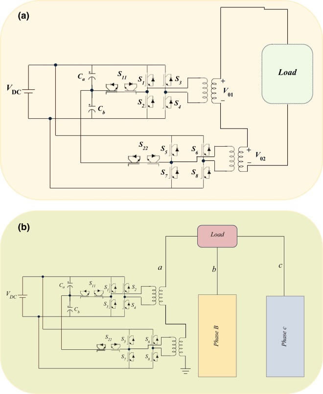
Coming to the details of proposed version, Fig. 5a and Fig. 5b demonstrates the single-phase and three-phase stacked cascade multilevel inverter architecture. Aforesaid it is the combination of SMC and CHB. We can observe an H-Bridge cell is attached to another cell which constitutes two semiconductor devices. Further, single-phase transformers are employed on the secondary side of each H-Bridge cell. By employing transformers to cascade multilevel inverter it can easily operate with single-DC source. However, if there is a variable frequency load, then separate DC source is must. Further, the reader should remember asymmetrical structures of CMI because, herein, the operation of the proposed version is similar to asymmetrical CMI. When we look at the operation of asymmetrical CMI, inputs of CMI are supplied with different ratios. Due to this fact, output voltage quality is predominantly improved. However, in the proposed version, due to presence of inner cell and capacitors, input voltage to H-bridge cell will be varied. Thus, H-bridge is supplied by different DC voltages at different instants. However, the capacitors and additional cell inside the proposed structures make architecture most reliable.
|
|
|
Fig. 5. (a) Details of single-phase SCMI. (b) Details of three-phase SCMI.
|
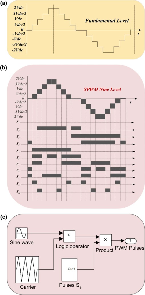
Further, to explain the principle of operation, lets consider Fig. 6 , which presents the key waveform for the proposed version. The presence of single DC source and capacitors facilitates different voltages at the output. However, capacitors play a key role in the proposed version operation. In fact it splits the DC voltage at different switching instance. To clear this point, consider the first level, i.e. Level 1 , switching states of first level for positive half cycle as presented in Table 1 . By switching S11 , S4 , S5 and S6 positive voltage VDC /2 is achieved at the output end. However, it can be observed that, this is the voltage which is handled by the top capacitor. Further, by switching S1 , S4 , S5 and S6 voltage VDC is retrieved at the output side of transformers, and this is the Second-Level of the proposed version. Herein, we should know that switching adjacent switches will compose converter voltage to zero, i.e. S5 and S6. In fact, this case restricts the second bridge to operate in the proposed version. In similar fashion, for the Third-Level , by switching S1 , S4 , S22 and S8 appropriately, 3VDC /2 voltage can be achieved. Finally, switching of S1 , S4 , S5 and S6 , 2VDC can be retrieved at the secondary side of transformers. All these switching states with the terminal voltages at each point of transforms are given in Table 1 . Further, to achieve the negative half cycle, switching states are presented in Table 2 . This is all about theoretical background of the proposed version. Further, the proposed design is verified with sinusoidal pulse width modulation technique (SPWM). To demonstrate the PWM technique for the proposed version, PWM control is shown in Fig. 6b . On inspecting the PWM control, every reference sin-wave and carrier waveform is compared with logic operator. Output of the logic operator is high frequency PWM waveform. This high frequency PWM output is multiplied with corresponding switching pulse. Thus one can achieve PWM pulses for matching time period of switch. By adopting this control for all respective switching pulses, PWM output can be obtained for the proposed SCMI. To validate the concept of round control technique and PWM switching approach, adequate simulation and experimentation is carried out. This is presented in the next section.
|
|
|
Fig. 6. (a) Key waveforms for proposed SCMI. (b) Key waveforms for proposed SCMI with SPWM. (c) SPWM control circuit.
|
| Output levels (n) | Switching conditions | Terminal voltage | Output voltage | ||||||||||
|---|---|---|---|---|---|---|---|---|---|---|---|---|---|
| S1 | S2 | S3 | S4 | S11 | S5 | S6 | S7 | S8 | S22 | V01 | V02 | V0 | |
| 0 | 1 | 1 | 0 | 1 | 0 | 1 | 1 | 0 | 0 | 0 | 0 | 0 | 0 |
| 1 | 0 | 0 | 0 | 1 | 1 | 1 | 1 | 0 | 0 | 0 | VDC /2 | 0 | VDC /2 |
| 2 | 1 | 0 | 0 | 1 | 0 | 1 | 1 | 0 | 0 | 0 | VDC | 0 | VDC |
| 3 | 1 | 0 | 0 | 1 | 0 | 0 | 0 | 0 | 1 | 1 | VDC | VDC /2 | 3VDC /2 |
| 4 | 1 | 0 | 0 | 1 | 0 | 1 | 0 | 0 | 1 | 0 | VDC | VDC | 2VDC |
| Output levels (n) | Switching conditions | Terminal voltage | Output voltage | ||||||||||
|---|---|---|---|---|---|---|---|---|---|---|---|---|---|
| S1 | S2 | S3 | S4 | S11 | S5 | S6 | S7 | S8 | S22 | V01 | V02 | V0 | |
| 0 | 1 | 0 | 0 | 1 | 0 | 0 | 0 | 1 | 1 | 0 | 0 | 0 | 0 |
| 1 | 0 | 1 | 0 | 0 | 0 | 0 | 0 | 1 | 1 | 0 | −VDC /2 | 0 | −VDC /2 |
| 2 | 0 | 1 | 1 | 0 | 0 | 0 | 0 | 1 | 1 | 0 | −VDC | 0 | −VDC |
| 3 | 0 | 1 | 1 | 0 | 0 | 0 | 1 | 0 | 0 | 1 | VDC | VDC /2 | −3VDC /2 |
| 4 | 0 | 1 | 1 | 1 | 0 | 1 | 1 | 1 | 0 | 0 | VDC | VDC | −2VDC |
4. Simulation and experimental validations
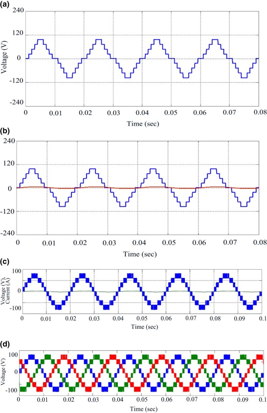
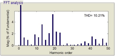
The proposed version is simulated in Matlab-Simulink. For the validation, R-L load is taken and the complete details of parameters are given in Appendix . Fig. 7a articulates the simulation validation of proposed SCMI. It is evident that voltage waveform is framed with nine-levels and further, Fig. 7b demonstrates the voltage and current waveforms for the proposed version. Fig. 8 presents the FFT spectrum for the proposed version. From the spectrum it is observed that lower order harmonics are significantly reduced. Total Harmonic Distortion (THD) is about 10.21%.
|
|
|
Fig. 7. (a) Simulation validation of proposed nine-level inverter. (b) Simulation validation of output voltage and current for proposed nine-level inverter. (c) Details of output voltage for proposed SCMI with SPWM. (d) Simulation validation of three phase output voltage with SPWM.
|
|
|
|
Fig. 8. Details of FFT spectrum for output voltage with round control method.
|
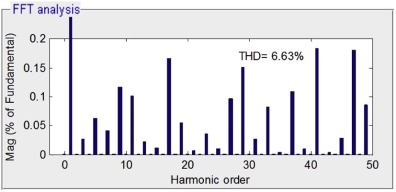
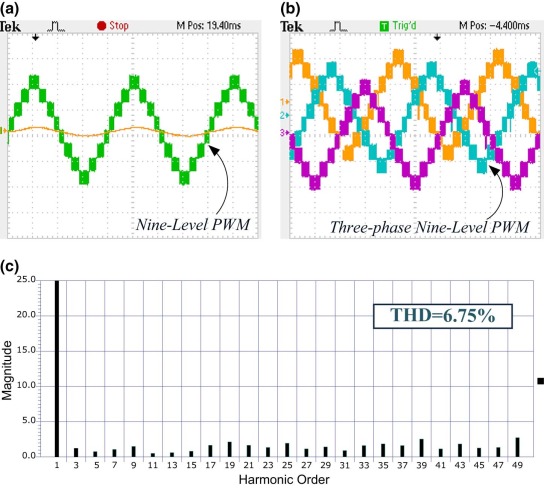
Further, to improve the performance of the proposed version SPWM approach is carried out. Key waveforms for the SPWM approach is demonstrated in Fig. 6b . Control technique to adopt PWM is presented in Fig. 6c . Later, single and three phase nine-level PWM output is shown in Fig. 7c and Fig. 7d . The FFT spectrum presented in Fig. 9 shows elimination of lower harmonics and THD is about 6.6%. Here one of the noticeable points is switching frequency. In the present case it is maintained at 1.5 kHz. With very low switching frequency performance is excellent.
|
|
|
Fig. 9. Details of FFT spectrum for output voltage with SPWM.
|
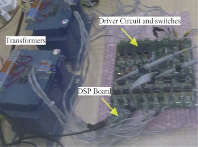
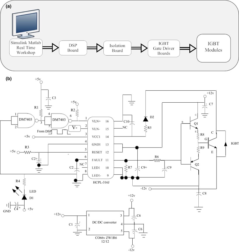
To validate the simulation findings, prototype validations are carried out in the laboratory. For the experimentation DSP based module was used. An analog expansion daughter board is interfaced between the DSP module and insulated gate bipolar transistor (IGBT) inverter. To program the DSP, distinct software packages are used in Matlab. In Matlab the program is written, and with the help of Matlab-Simulink the program is configured to run the DSP. Later, in the proposed circuit topology, Fairchild semiconductors FGH20N60UFD based IGBTs are used. Fig. 10 indicates the construction of the proposed version by employing transformers. The measured quantities are the load currents, load voltages, which are measured with hall-effect voltage and current transducers. Input DC voltage is taken as 120 V and for transformers, transformation ratios are taken as 1:1. With the help of DSP, switching signals are generated. Target output voltage is 230 VAC . Further, details of gate drive circuit of HCPl-316J are presented in Fig. 11 .
|
|
|
Fig. 10. Details of hardware setup for the proposed stacked cascaded multilevel converter with single-phase transformers.
|
|
|
|
Fig. 11. (a) Control architecture for proposed multilevel inverter. (b) Details of Gate Drive Circuit.
|
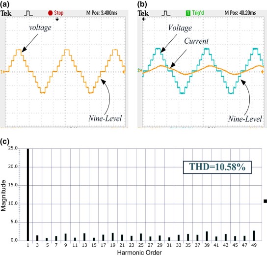
Coming to the validations, Fig. 12a highlights the performance of proposed SCMI. As only two bridge cells are used nine level output is achieved. However, this is in close agreement with Fig. 7a . Later, Fig. 12b demonstrates voltage and current waveforms of proposed CMI. Further, on observing current waveform ripple content is nullified and waveform is smooth in nature. Fig. 12c presents the details of the FFT spectrum for output voltage of the proposed version. THD is about 10.8%. Herein readers should note that FFT validation is just to identify the output quality. However, to achieve this quality we have not used any switching algorithms like selective harmonic elimination pulse width modulation methods (SHEPWM). Aforementioned this performance is achieved with round control technique.
|
|
|
Fig. 12. (a) Output voltage (scale: 120 V/div), Time scale: 5 ms. (b) Output voltage (scale: 120 V/div), output current (scale: 3 A/div), Time scale: 5 ms. (c) Experimental FFT spectrum for proposed SCMI.
|
Fig. 13 demonstrates single and three-phase verifications for the proposed version with SPWM, on observing Fig. 13a and Fig. 13b are in close agreement with Fig. 7c and Fig. 7d . The FFT spectrum shown in Fig. 13c is also very close to the simulation verifications. Thus, from theoretical findings and experimental results, the proposed version has been fruitfully verified. But to show some of the merits of the proposed version, a comparative study is carried among the traditional and the proposed version. This is presented in the next section.
|
|
|
Fig. 13. (a) PWM Output voltage (scale: 120 V/div), output current (scale: 3 A/div), Time scale: 5 ms. (b) PWM Output voltage (scale: 120 V/div), Time scale: 5 ms. (c) Experimental FFT spectrum for proposed SCMI.
|
5. Comparative study
To show the merits of suggested architectures a comparative approach is carried out among the traditional multilevel inverters. Table 3 shows the comparative study, whereby the comparative approach is done with NPC, FC and CMI based inverter. In general, to produce a nine-level phase voltage from an NPC, FC and CMI require at least 16 semiconductor switches [16] , whereas in the proposed version, the number of switches used is only 12. Further, like NPC and FC, extra clamping diodes and balancing capacitor are not required. Another remarkable issue is DC-Bus count; in suggested versions it is only one, whereas in traditional cases it is 8, 8 and 4 for NPC, FC and CMI respectively. Thus from this comparison we can conclude that the suggested version uses less number of switching components to produce the same number of output levels.
| Type/Item | Switch | Clamping diode | Balancing capacitor | DC-Bus |
|---|---|---|---|---|
| Diode clamped | (m − 1) × 2 | (m − 1) × (m − 2) | NA | (m − 1) |
| 16 | 56 | 8 | ||
| Flying capacitor | (m − 1) × 2 | NA | [(m − 1) × (m − 2)]/2 | (m − 1) |
| 16 | 28 | 8 | ||
| Cascaded FB-cell | (m − 1) × 2 | NA | NA | (m − 1)/2 |
| 16 | 4 | |||
| Suggested SCMI | 10 | NA | NA | 1 |
6. Conclusion
In this paper we suggested a stacked cascade multilevel inverter by employing single-phase transformers. The suggested inverter uses only one power source for each phase while producing desired voltage waveforms. In addition, the suggested version uses much less number of semiconductor devices when compared to other multilevel based architectures. Thus the suggested SCMI serves as reliable and cost effective converters. Moreover as less number of components is used, size of equipment drastically comes down. The presented SCMI based topologies are verified with hardware prototype setup. Adequate results are presented to confirm the findings. Thus from the above findings new evolution of technical requirements are fulfilled.
Appendix
| Items | Specifications and features |
|---|---|
| Kilovolt ampere rating | 2 KVA |
| Transformers | EI Lamination 1:1 ratio |
| DSP | To generate switching signals |
| Line to line voltage | Nine level, 220 V |
| Current sensor | LTS 25-NP 25 A |
| Voltage sensor | LV 25P-1200 V |
| Load | R-L load |
| Sample time | 50 micro µs |
References
- [1] J. Ebrahimi, E. Babaei, G.B. Gharehpetian; A new multilevel converter topology with reduced number of power electronic components; IEEE Trans. Ind. Electron, 59 (2) (2012), pp. 655–667
- [2] Y. Cho, T. LaBella, J.-S. Lai, K. Senesky; A carrier-based neutral voltage modulation strategy for multilevel cascaded inverters under unbalanced DC sources; IEEE Trans. Ind. Electron, 61 (2) (2014), pp. 625–636
- [3] J.-M. Shen, H.-L. Jou, J.-C. Wu, K.-D. Wu; Five-level inverter for renewable power generation system; IEEE Trans. Energy Convers, 28 (2) (2013), pp. 257–266
- [4] J. Dixon, J. Pereda, C. Castillo, S. Bosch; Asymmetrical multilevel inverter for traction drives using only one dc supply; IEEE Trans. Vehicular Technol, 59 (8) (2010), pp. 3736–3743
- [5] Y. Ye, K.W.E. Cheng, J. Liu, K. Ding; A step-up switched-capacitor multilevel inverter with self-voltage balancing; IEEE Trans. Ind. Electron, 61 (12) (2014), pp. 6672–6680
- [6] Y. Suresh, A.K. Panda; Research on cascade multilevel inverter by employing three-phase transformers; IET Power Electron, 5 (5) (2012), pp. 561–570
- [7] P. Lezana, J. Rodriguez, D.A. Oyarzun; Cascade multilevel inverter with regeneration capability and reduced number of switches; IEEE Trans. Ind. Electron, 55 (3) (2008), pp. 1059–1066
- [8] E. Babaei; Optimal topologies for cascaded sub-multilevel converters; J. Power Electron, 10 (3) (2010), pp. 251–261
- [9] Y. Suresh, A.K. Panda; Investigation on hybrid cascade multilevel inverter with reduced DC source; Renew. Sustain. Energy Rev, 26 (2013), pp. 49–59
- [10] N.A. Rahim, M.F.M. Elias, W.P. Hew; Transistor-clamped H-bridge based cascaded multilevel inverter with new method of capacitor voltage balancing; IEEE Trans. Ind. Electron, 60 (8) (2013), pp. 2943–2956
- [11] A. Masaoud, H.W. Ping, S. Mekhilef, A.S. Taallah; New three-phase multilevel inverter with reduced number of power electronic components; IEEE Trans. Power Electron, 29 (11) (2014), pp. 6018–6029
- [12] G. Gateau, T.A. Meynard, H. Foch; Stacked multicell converter (SMC): properties and design; IEEE 32nd Annual Power Electronics Specialists Conference, PESC 2001, June 17-22, Vancouver, Canada (2001)
- [13] B. McGrath, D.G. Holmes; Analytical determination of the capacitor voltage balancing dynamics for three phase flying capacitor converters; IEEE Trans. Ind. Appl, 45 (4) (2009), pp. 1425–1433
- [14] G. Gateau, T.A. Meynard, H. Foch; Stacked multicell converter (SMC): control and natural balancing; IEEE 33nd Annual Power Electronics Specialists Conference, PESC 2002, June 23-27, Queensland, Australia (2002)
- [15] M. Rotella, G. Peñailillo, J. Pereda, J. Dixon; PWM method to eliminate power sources in a nonredundant 27-level inverter for machine drive applications; IEEE Trans. Ind. Electron, 56 (1) (2009), pp. 194–201
- [16] F.S. Kang, S.J. Park, S.E. Cho, C.U. Kim, T. Ise; Multilevel PWM inverters suitable for the use of stand-alone photovoltaic power systems; IEEE Trans. Energy Convers, 20 (4) (2005), pp. 906–991
Document information
Published on 10/04/17
Licence: Other
Share this document
Keywords
claim authorship
Are you one of the authors of this document?

